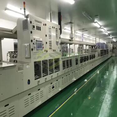
What are the steps in PCB etching?
PCB (Printed Circuit Board) etching is a crucial step in the manufacturing process of PCBs, where unwanted copper is selectively removed to create the desired circuit traces. The etching process involves several steps, and here's a detailed overview of each stage:
1. Design and Layout: Before etching can begin, the PCB design must be finalized using computer-aided design (CAD) software. This design includes the placement of electronic components, the routing of copper traces, and the locations where etching will occur.
2. Material Selection: Choose the appropriate PCB substrate material, typically a fiberglass-reinforced epoxy laminate with a thin layer of copper laminated onto one or both sides.
3. Resist Application:
Clean the Copper Surface: Ensure that the copper surface of the PCB substrate is clean and free of contaminants. Any grease, dust, or oxidation can affect the quality of the resist adhesion.
Apply Resist: A photosensitive resist material is applied to the entire surface of the PCB. This resist material can be applied using various methods, such as screen printing, roller coating, or spray coating. Some PCBs use a dry film resist that is laminated onto the copper surface.

4. Exposing the PCB:
Masking: Cover the areas where you want to retain the copper traces with a mask or a film. This mask can be a photomask for photolithographic processes or a simple stencil for other methods.
Exposure: Expose the PCB to ultraviolet (UV) light through the mask. The resist material undergoes a chemical change when exposed to UV light, creating a pattern that corresponds to the desired copper traces.
Developing: After exposure, the PCB is immersed in a developer solution that removes the unexposed resist, leaving behind the pattern of resist that will protect the copper traces during etching.
5. Etching:
Preparing the Etchant: Prepare the etchant solution, which is typically a chemical like ferric chloride or ammonium persulfate. The etchant reacts with exposed copper, dissolving it.
Immersion: Submerge the PCB in the etchant solution. Agitate the solution to ensure even etching. The etching process may take several minutes to complete, depending on the design and thickness of the copper.
Monitoring: Continuously monitor the progress of the etching to ensure that all unwanted copper is removed. The resist material protects the copper traces, preventing them from being etched.
6. Cleaning and Neutralization:
Removing the PCB: Once etching is complete, remove the PCB from the etchant solution.
Neutralization: Rinse the PCB thoroughly with water to remove any residual etchant. Submerge it in a solution that neutralizes any remaining etchant and stops the etching process.
7. Resist Removal:
Cleaning: Use a solvent or chemical stripper to remove the remaining resist material from the PCB surface.
Rinsing: Rinse the PCB again to remove any traces of the resist stripper and neutralizer.
8. Inspection and Quality Control:
Visual Inspection: Examine the PCB for any defects, shorts, or irregularities in the copper traces. Touch up or repair any issues as needed.
Testing: Conduct electrical tests to ensure that the copper traces have the desired conductivity and that there are no unintended connections.
9. Final Finishing:
Surface Finish: Apply a suitable surface finish, such as solder mask and solder plating, to protect the copper traces and facilitate component soldering.
Drilling: If needed, drill holes for mounting components or creating vias.
10. Final Inspection: Perform a final inspection to verify that all components are correctly placed and that the PCB meets the required specifications.
Once these steps are completed, the PCB is ready for assembly with electronic components, forming an integral part of various electronic devices and systems. The etching process is a critical and precise step that determines the functionality and reliability of the final PCB.
- Previous: Choosing the Right Tire Shredder Machine
- Next: What is a CO2 Tank Used For?

